The requirements for this power supply differs greatly from the supply for the pulsed thruster in that it is necessary to closely regulate the power delivered to the arc. I chose an operating power of approximately 12 kW based on the available wall power available - in this case a single phase of 240 VAC at 50 A, only moderately larger than the 240 VAC 30 A usually available for clothes dryers and other appliances in many US households. Based on previous experience, I anticipated an arc voltage somewhere in the range of 30-60V, which would require an arc current of 400-200 A, respectively. Background In this case I designed the power supply around a switching converter for small size and high efficiency. Specifically, I chose the full bridge soft switching topology due to its ability to handle high power levels with maximum efficiency. This topology is a derivative of the buck converter topology, shown below. 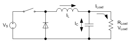 Fig. 1: Buck Converter The switch is controlled using pulse width modulation (PWM) in order to generate a square waveform with an average value equal to the desired output voltage. The inductor and capacitor form a filter which removes most of the switching component, resulting in a nearly constant output voltage equal to the source voltage VS multiplied by the duty ratio D. The output current is then equal to the output voltage divided by the load resistance. This application is different in that the load is no longer a constant resistance, but a highly non-linear arc. The characteristics of the arc make the output capacitor unnecessary. 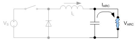 Fig. 2: Buck Converter Supplying an Arc Due to the ability of the arc to conduct very large currents with little change in voltage, the capacitor will not provide any useful filtering as it would with a resistive load. Instead, the capacitor will maintain the voltage of the arc and neither accept nor supply any current. 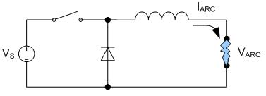 Fig. 3: Buck Converter for Supplying an Arc Load As a result, the capacitor can be removed entirely. In this configuration, the arc current is maintained within some limits by the inductance, and the load voltage is determined by the arc's V-I curve. At higher currents, the arc's voltage tends to remain relatively constant over a wide range of currents, resulting in a relatively constant load voltage. The duty cycle for the modified circuit in Fig. 3 is the same as for the traditional buck converter shown in Fig. 1. 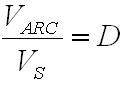 Eq. 1: Duty Cycle Relationship for Modified Buck Topology The full bridge topology is very similar in operation, but uses a transformer in order to allow a much wider range of output voltages and to provide isolation between the source and load. The additional switches and diodes are included in order to allow the transformer to operate correctly. Fig. 4 shows one possible configuration of the full bridge topology for the purpose of clarity. 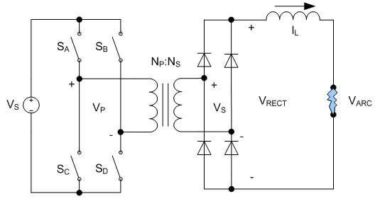 Fig. 4: Full Bridge Converter Topology The transformer requires a bidirectional voltage in order to avoid saturation of the magnetic core, which is generated by the switches SA - SD, operated in pairs. First switches SA and SD are turned on, applying a positive voltage to the transformer. These switches are turned off and after a delay switches SB and SC are turned on, applying a negative voltage to the transformer. This AC square wave is then rectified by the four diodes on the transformer's secondary, generating a positive square wave which is identical to that generated by the buck converter shown in Fig. 3.  Additional info - read more about
the phase shifted full bridge converter here. [1]
Additional info - read more about
the phase shifted full bridge converter here. [1]In practice the full wave rectifier shown in Fig. 4 is usually substituted with a circuit consisting of fewer diodes in order to reduce losses; however, the concept is similar. Additionally, the switching pattern for the two pairs of switches can be modified to allow lossless switching, but again, the concept is similar. The relationship between the source and arc voltage is similar to that shown in Eq. 1, with the addition of a term to account for the effect of the turns ratio of the transformer. 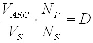 Eq. 2: Duty Cycle Relationship for Full Bridge Topology The voltages and currents generated by the full bridge converter are shown below. 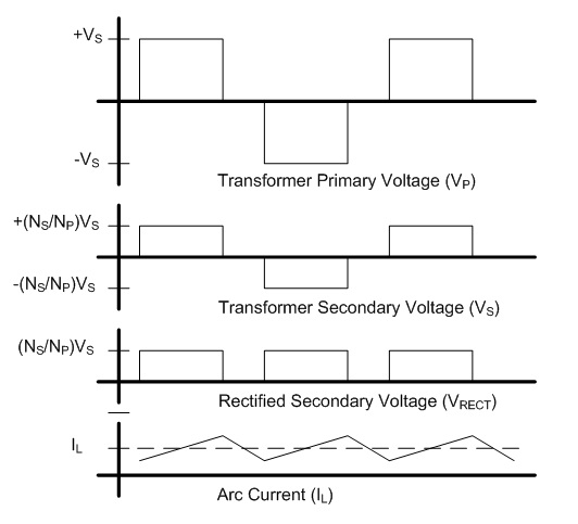 Fig. 5: Full Bridge Waveforms (Fig. 4 circuit) Note that these waveforms apply specifically to the circuit shown in Fig. 4, and are shown as an introduction to the concepts that are applied to other circuit configurations. The full bridge rectifier is not frequently used, due to the number of diodes and the losses associated with them. A more popular rectification method is to employ a center-tapped secondary and full wave rectification. This halves the number of diodes needed at the expense of a slightly larger and more difficult to manufacture transformer secondary, but otherwise operates identically to the circuit in fig. 4. 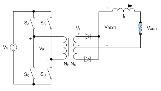 Fig. 6: Center-Tapped Secondary with Full Wave Rectification Another arrangement exists which does not require a center-tapped secondary winding at the expense of an additional filter inductor and complexity. This is known as the current doubler rectifier. 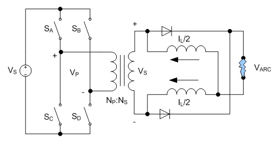 Fig. 7: Current Doubler Rectifier The operation and advantages of this circuit are not necessarily apparent at first glance; however, this allows reduced currents in the transformer's secondary in addition to eliminating the center tap. The addition of a second inductor can also be helpful, especially in high current applications where the thermal load is spread across several components. Furthermore, the current ripples in the two inductors are out of phase and partially cancel each other out, and therefore reduce the magnitude and increase the frequency of the ripple allowing for smaller inductors in many instances. The elimination of the center tap in the secondary transformer winding requires a modification to the duty cycle calculation.  Eq. 3: Duty Cycle Calculation for Full Bridge with Current Doubler Rectifier
Additional Info - read more about
the current doubler rectifier here. [2]Magnetics Design The design process was performed iteratively in a Microsoft Excel spreadsheet in order to optimize the design quickly; however, the process described here will use only the final design values for clarity. The spreadsheet developed for this design is available at the bottom of this page, along with additional design files. The first step in performing the design is to determine the major operating parameters, i.e. the input and output conditions. The input will be taken from a rectified single phase 240 VAC, which will have a DC value of  .
A maximum operating power of 4 kW
per converter with three converters operating in parallel was chosen,
which requires 11.7 A from the DC bus per converter. The output voltage
is estimated to be between about 30 - 60 V, which requires 133 - 66.7 A
per converter respectively.
Since the current doubler rectifier uses two inductors which share the
output current evenly, the maximum average DC current through each
inductor will be 66.7A. .
A maximum operating power of 4 kW
per converter with three converters operating in parallel was chosen,
which requires 11.7 A from the DC bus per converter. The output voltage
is estimated to be between about 30 - 60 V, which requires 133 - 66.7 A
per converter respectively.
Since the current doubler rectifier uses two inductors which share the
output current evenly, the maximum average DC current through each
inductor will be 66.7A. The next step is to choose a turns ratio for the transformer which allows the maximum output voltage of 60 V to occur at a high duty cycle. This should coincide with a duty ratio of around 0.8 to 0.9 in order to allow some headroom to allow for responding to transients. In a full bridge converter with a full wave rectifier a turns ratio of 5:1 would yield a duty cycle of 0.882, but since the current doubler rectifier only carries half of the load current at the transformer secondary the transformers secondary must have twice the voltage, requiring a turns ratio of 5:2, which can be calculated from Eq. 3. The worst case for the transformer core flux density occurs at peak VOUT, in this case corresponding to an arc voltage of 60 V and a D of 0.882. The core flux is computed as the applied volt-seconds divided by the number of primary turns, and the flux density is computed as the core flux divided by the core cross sectional area. Therefore, the core flux density is calculated as  Eq. 4: Flux Density in the Transformer Core Where B is the peak flux density in the core VIN is the input voltage to the converter in Volts fs is the switching frequency in Hertz NP is the number of primary turns on the transformer AC is the transformer core cross sectional area in square meters With an input voltage of 340 V, duty cycle of 0.883, switching frequency of 60 kHz, 30 primary turns, and a core cross section of 626 mm2 the core flux density will be 0.133 T (divide the result of Eq. X by 106 to correct for the core cross section being given in mm2.) There is plenty of margin, since the material saturation flux density for my core is closer to 0.35 T. Next, the worst case for the inductor core flux density occurs at the lowest arc voltage because this corresponds to the highest instantaneous inductor current. The average inductor current and the current ripple must be known first. The average inductor current is calculated by dividing the output power by the arc voltage and dividing that result by two, since the arc current is split evenly between the two inductors.  Eq. 5: Average Inductor Current Where IL_AVG is the average inductor current in each of the two inductors in Amps PIN is the maximum input power in Watts VARC is the arc voltage in volts  is the converter's
efficiency is the converter's
efficiencyWith an input power of 4,000 W, an efficiency of 100%, and an arc voltage of 30 V the average inductor current will be 66.7 A. Next, the inductor ripple must be calculated. The ripple on each inductor is equal to the Volt-seconds applied to it divided by the inductance. Since this design uses a current doubler rectifier, positive pulses from the transformer will be applied to one inductor and negative pulses to the other. The means that each inductor has the transformer output voltage applied to it for a duration of D times the full switching cycle time on alternate cycles. The current ripple will therefore be 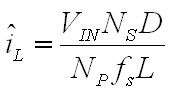 Eq. 6: Peak to Peak Inductor Ripple Current Where L is the inductance of the filter inductor in Henries. With an input voltage of 340 V, 12 secondary turns, D equal to 0.441 (for VARC of 30 V), 30 primary turns, 60 kHz switching frequency, and 30.4 uH inductance the peak to peak ripple current will be 32.9 A. Therefore, the peak inductor current will be equal to the average current plus half of the ripple current, equal to 83.2 A. Based on this result, the peak inductor core flux can be calculated as 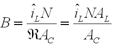 Eq. 7: Inductor Peak Flux Density Where  is the peak
inductor current in
Amps is the peak
inductor current in
AmpsN is the number of turns on the inductor  is the
reluctance of the core is the
reluctance of the coreAC is the cross sectional area of the core in m2 AL is the core factor in H/sqrt(t) With a peak inductor current of 83.2 A, 13 turns on the inductor, an AL of 180x10-9, and a cross section of 540 mm2 the peak inductor flux density is 0.36 T (multiply results from Eq. X by 106 to correct for AC being given in mm2.) Note that and AL
are inverses of each
other, and the peak core flux density can be calculated with either
value, whichever is handy. AL
is frequently
given in ferrite core data
sheets, while is typically calculated based on
geometries. At this point it is easy to calculate the ripple current seen by the arc, which is different than the ripple of the individual inductors. Since the current ripple of the two inductors is out of phase, they partially cancel. The cancellation factor is given by 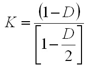 Eq. 8: Current Ripple Cancellation Factor D is equal to 0.441 at the minimum arc voltage, yielding a cancellation factor of 0.717. To obtain the arc current ripple, multiply the individual inductor ripple magnitude (32.9 A) by the cancellation factor. This results in an arc current ripple of 23.6 A out of a total current of 133 A, or about 17.7%.
Additional
Info - Read more about current cancellation in the current doubler
rectifier here.
[3]Next, losses in the transformer and inductors will be considered, starting with the inductor. The magnetic core losses are the most straightforward, so those will be calculated first. The losses in the inductor core are a function of the magnitude and frequency of the flux density ripple. Eq. 7 can be used to calculate the flux density ripple in the same way it was used to calculate the peak flux density. With an inductor current ripple of 32.9 A and parameters as described before, the flux density ripple magnitude is calculate to be 0.142 T. For archaic reasons most magnetic material datasheets use the flux density ripple divided by two, so 71 mT is the actual value to use to calculate the core loss. Also, since the inductors in a current doubler rectifier receive alternate pulses, the frequency is half of the switching frequency, 30 kHz is used to calculate the loss instead of 60 kHz. The last number required for the core loss calculation is the core volume, which is 1.08 x 10⁻⁴ m3. The core material is Ferroxcube 3F3. The datasheet for that material can be found here. The curve for 25 kHz is closest to the actual inductor frequency of 30 kHz, so we find where that curve intersects the vertical line for 70 mT and then read off the position on the vertical axis. In this case, the value is off the bottom edge of the chart, so I chose to use 10 kW/m3, which is close to the actual value if the manufacturer's curves were extended. Multiplying this value by the volume of the core gives a core magnetic loss of 1.08 W. The inductor copper losses are calculated next. In this case, the inductor is constructed of 13 turns of 5 mil thick copper foil 38 mm wide. A E65/32/27 core is used (datasheet here) with a CP-E65-1S-T bobbin (described in the same document.) The average length of a turn on this bobbin is 150 mm, which allows the total length of the copper foil need to be calculated by multiplying the average turn length by the number of turns, resulting in a strip with a length of 1.95 m. The DC resistance of this conductor can be calculated by using the equation 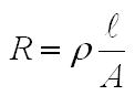 Eq. 9: Resistance of a Conductor Where  is the
resistivity of the conductor material in is the
resistivity of the conductor material in  ( ( for copper) for copper) is the length of the conductor in meters is the length of the conductor in metersA is the cross-sectional area of the conductor in m2 With a resistivity of , length
of 1.95 m, cross-sectional area of 4.83 mm2,
the DC
resistance of the strip will be 6.79 mΩ (don't forget to correct for
the units.) The effective resistance of the winding will be higher with
AC currents due to skin and proximity effects. First, the skin depth
needs to be calculated for these conditions.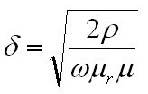 Eq. 10: Skin Depth in a Conductor where  is the skin depth,
  is the
resistivity of the conductor ( is the
resistivity of the conductor (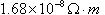 for copper) for copper)  is the
permeability of free space (equal to is the
permeability of free space (equal to  for
most non-magnetic materials) for
most non-magnetic materials) is the
relative permeability of the conductor (approximately 1 for most
non-ferrous conductors.) is the
relative permeability of the conductor (approximately 1 for most
non-ferrous conductors.) With ω equal to 2π30 kHz, the skin depth is 0.377 mm. The AC resistance for the fundamental frequency (30 kHz) can be determined from the Dowell plot. 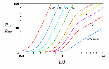 Fig. 8: Dowell Plot Showing AC Resistance Increase With Skin Depth where h is the height of the conductor, 5 mils equal to 0.127 mm. The ratio of the conductor height to skin depth is then 0.177 / 0.377, or 0.337. Following the curve for the nearest number of turns (10 on the chart) at 0.4 on the horizontal axis the ratio of AC resistance to DC resistance is roughly 1.3. This means that the resistance at 30 kHz is 1.3 times higher than the DC resistance. Since the chart is only calibrated for sinusoidal currents, and the saw-tooth waveform in the inductor has higher frequency harmonics which will be subjected to even higher resistances, a rough estimate of the overall losses can be calculated by multiplying the final result by a factor of 1.4. This yields a total resistance of 6.79 mΩ times 1.3 times 1.4 equal to 8.82 mΩ. Next the RMS value for the inductor current must be determined. This current is a saw-tooth waveform with a DC offset.  Fig. 9: Inductor Current Waveform The RMS value for this waveform is given by the equation 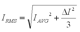 Eq. 11: RMS Current for a Saw-Tooth Waveform With an IAVG of 66.7 A and ripple of 32.9 A the RMS value is 69.3 A. The copper losses for the inductor are then calculated as IRMS2R, equal to 59.4 W. Adding the core loss gives a total loss of 60.5 W per inductor. The temperature rise can then be roughly estimated based on a rule of thumb which states that the thermal resistance under natural convection is approximately 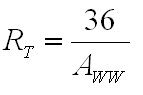 Eq. 12: Thermal Resistance of an E Core where AWW is the area of the winding window of the E core in cm2. The winding window can be calculated from the datasheet values, equal to 493 mm2. The thermal resistance under natural convection is then 7.3 C/W. Forced convection can reliably reduce this resistance by a factor of 10, so 0.73 C/W can be achieved using a fan. Multiplying the thermal resistance by the power dissipation gives the inductor temperature rise above ambient, equal to 44.1 C. The inductor temperature with 25 C ambient would then be 69.1 C. The transformer core and copper losses can be treated identically to determine the total loss and temperature rise with a few small modifications. First, the core flux density of the transformer is not determined by the current flowing through it, but by the applied volt-seconds. With a 30 V arc the flux density swing will be 0.133 T; again, using half of that value for archaic reasons, or 66 mT. Since positive and negative voltage pulses are applied to the transformer alternately, the actual frequency of the flux is half the switching frequency, so use 30 kHz here too. The transformer core material is different from the inductor, in this case TDK H7C2 material. Curves for this material do not appear to be available, but Magnetics F material is listed as an equivalent, so the published equations for that material were used to determine a core loss of 1.17 W. The copper losses for the transformer are calculated similarly, but the current waveforms are somewhat different and the primary and secondary windings need to be considered separately. First, consider the current waveform of the secondary winding. During the TON interval the transformer secondary carries only the ramping current from the active inductor. There is a free-wheeling interval that follows the TON interval when there is no secondary voltage, and the load voltage causes the current to ramp down. This sequence is then repeated at the other inductor during the next TON interval when the transformer secondary voltage reverses. 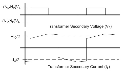 Fig. 10: Transformer Secondary Winding Current To calculate the RMS value for the secondary's current the waveform must be considered as two separate parts, the RMS of each part must be calculated, and then the overall RMS value for the waveform can be computed. The two components of the secondary current are shown below, along with the equation for calculating the RMS value of the individual components. 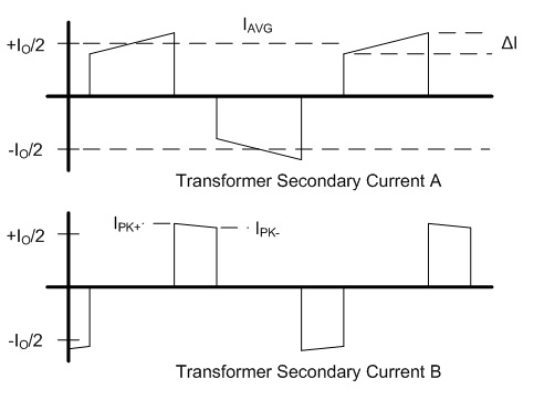 Fig. 11: Secondary Current Components for Calculating RMS Value 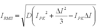 Eq. 13: RMS Value of a Trapezoidal Waveform Since the low arc voltage condition (30 V) is being considered, D is 0.441. For the "A" waveform IAVG and ΔI are identical to the values used in the inductor calculations, 66.7 A and 32.9 A respectively. From this, the peak current can be calculated to be 83.2 A.Therefore, the RMS value of the "A" waveform is 44.7 A. The difference between IPK+ and IPK- is caused by the arc voltage being applied to the inductor for the remainder of the switching period, and can be calculated to be 9.19 A. Using these values in Eq. 13 for the "B" waveform yields an RMS value of 58.8 A. These two values can then be combined in to an overall RMS value by using Eq. 14. 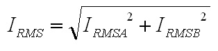 Eq. 14: Combining RMS Values Accordingly, the combined RMS values of the "A" and "B" parts of the secondary current waveforms yield an overall RMS value of 73.7 A. Using the same process as for the inductor, the copper losses for the transformer secondary winding can now be calculated. With 12 turns of 8 mil copper foil, 62 mm foil width and 161 mm mean length of a turn the DC resistance is equal to 2.58 mΩ. The skin depth to conductor thickness ratio is 0.54, yielding a 2.3 AC resistance multiplier and an AC resistance of 5.93 mΩ. The I2R loss for the secondary winding of the transformer (including a factor of 1.4 for higher losses from harmonic content) is then 45.1 W. The primary winding is treated identically. First, the shape of the primary current waveform is established. During the TON period the secondary current is reflected back to the primary by the turns ratio, and during the remainder of the switching period the primary current freewheels near the peak primary current. 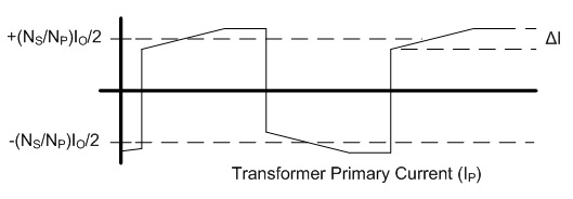 Fig. 12: Transformer Primary Current This gives an IAVG of 66.7 A times a turns ratio of 0.4, equal to 26.7 A. The reflected current ripple is calculated to be 13.2 A, and from that the peak current can be calculated to be 33.3 A. The primary current can then be separated into two components in order to calculate the RMS value. 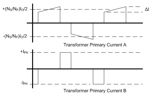 Fig. 13: Primary Current Components for Calculating RMS Value The "A" component RMS value can be calculated using Eq. 13 and the reflected secondary currents just calculated. This gives a result of 17.9 A. The equation for the "B" component is given by the equation 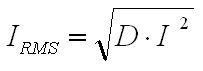 Eq. 15: RMS Value of a Square Wave The RMS value of the "B" component, with a duty cycle of 0.559 and a peak current of 33.3 A, is 24.9 A. The overall RMS value of the primary current is then 30.6 A. The primary winding consists of 30 turns of 2 mil copper foil 62 mm wide with a mean turn length of 161 mm. This corresponds to a DC resistance of 25.8 mΩ and a nearly identical AC resistance, with copper losses for the primary equal to 33.9 W. Totalling the core losses, secondary copper losses and primary copper losses yields a total dissipation of 80.2 W. From the core winding window area the natural convection thermal resistance is estimated at 3.02 C/W, and 0.302 C/W with forced convection. The estimated temperature rise for the core is then 24.2 C. Magnetics Construction Both the transformer and inductors are constructed using flat copper foil windings assembled onto bobbins around which the core is assembled. There are several considerations common to the construction of both parts. First, the copper foil is cut to allow 3 mm of clearance between the copper and the bobbin on each side. Next, each foil strip is wound along with a strip of Kapton film which is the exact width of the bobbin winding area. This provides both the turn to turn electrical insulation (since the copper foil is bare) and the winding to winding isolation required for safety. This provides a total creepage distance of 6mm between the primary and secondary windings, which prevents surges and spikes on the primary from propagating to the secondary. Also, both the transformer and inductors are encased in a varnish which serves as additional insulation, provides mechanical strength, and increases heat flow out of the parts. The first step is to cut the required lengths, widths, and thickness of of copper sheeting and Kapton film down to the proper dimensions. The copper is thin enough to cut accurately with a good pair of scissors, so the dimensions for each piece were measured out, marked with a straight edge and knife, and then cut to size. Fig. 14: Cutting Copper Sheeting to Size Next, the leads that connect to the copper strip on the inside of the winding are attached. This is accomplished using bundled magnet wire soldered to the beginning of the strip. The insulation on some magnet wire will peal back with the heat from soldering. For other types of insulation, it must be removed mechanically by scraping, or chemically removed. In this case I used a chemical stripper sold by the Eraser Company. The stripper comes as a solid, and is melted in a solder pot to activate it. The magnet wire is then inserted for a few seconds, and the insulation is dissolved. Fig. 15: Insulation Removal by Chemical Stripper Fig. 16: Attaching Transformer Lead to Copper Strip Once the lead is attached winding can begin. Start by taping down the Kapton strip on an outward face of the bobbin, and then tape the starting end of the copper strip over it. Fig. 17: Taping Kapton Insulation and Copper Strip to Bobbin Apply heat shrink tubing or Teflon tubing to the lead. Any conductor which passes through the 3 mm isolation gap must have secondary insulation. Fig. 18: Insulating Lead After the insulation and copper are taped down and the secondary insulation is added, wind the appropriate number of turns onto the bobbin. For square center legs, be sure the copper foil follows the edged by bending and pressing around every edge to get the winding as compact as possible. For circular center legs, be sure to wind the foil and insulation tightly. Fig. 19: Bobbin With Wound Coil, Circular and Square To terminate the winding, cut the copper foil and insulation to length and tape down the ends to prevent the coil from unwinding. Fig. 20: Taped Winding The second lead can now be soldered onto the coil, and insulated with shrink tubing or Teflon tubing. Fig. 21:Attaching Second Lead to Winding Next, apply several layers of insulation that extend completely from one side of the bobbin to the other. Kapton tape or polyester tape are both acceptable. Fig. 22: Insulate Winding With Tape For single coil inductors, the winding is complete. For transformers, or multi-winding inductors, wind each additional coil using the same procedure. Once the winding is completed assemble the core in the bobbin and tape around the outside of the core with polyester tape to secure the assembly. Fig. 23: Completed Assembly Optionally, the assembled parts can be dipped in varnish to provide additional insulation, mechanical strength, and improve heat transfer. I have not seen electrical grade varnishes and resins available anywhere except directly from the manufacturer, such as Dolph's, which is where I purchase from. Be sure to choose a resin that is intended for dipping, if that is your intention If you have appropriate equipment, you may choose to perform vacuum pressure impregnation (VPI) instead, which requires resins designed for that process. The idea is to dip the part in the resin in a vacuum, and then apply high pressure. This forces the resin to completely fill any voids that might have otherwise been allowed to remain. Fig. 24: VPI Process - Vacuum and Dipping, Applying High Pressure, Baking, Finished Product Measuring Magnetic Properties The phase shifted switching scheme that allows lossless switching uses the parasitic reactive components of the circuit, including those of the transformer. Therefore, it is important to properly identify the values of these elements in order to ensure proper operation of the lossless switching, and also to allow accurate modeling and simulations. The first parameter to identify is the leakage inductance of the transformer's primary and secondary windings. The leakage inductance is caused by flux that does not link both coils. This leakage inductance stores energy which is not transfered from the primary to the secondary, and often causes voltage spikes during switching. In an ideal transformer the impedance on the secondary is reflected back to the primary by the square of the turns ratio, so ideally a perfectly shorted secondary winding would cause the primary winding to see zero impedance as well. 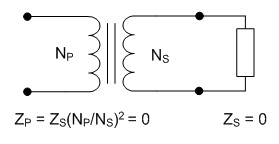 Fig. 25: Ideal Transformer With Shorted Secondary However, since the leakage inductance is not linked to the secondary, it is not shorted out, and remains in the circuit. 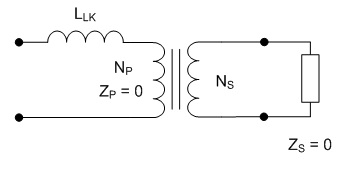 Fig. 26: Practical Transformer With Shorted Secondary Therefore, the primary leakage inductance can be measured by shorting out the secondary winding and measuring the inductance of the primary. The reverse can also be performed to measure the leakage inductance of the secondary winding. Using this method, the leakage inductance of the primary was determined to be uH, and the leakage inductance of the secondary was determined to be uH. Additionally, the magnetizing inductance of the transformer can be easily measured using an inductance meter. Simply measure the inductance of the primary winding with a meter, making sure the secondary is completely disconnected. For this transformer, the magnetizing inductance was measured to be uH. Note that this measurement includes the leakage inductance. Finally, the transformer's self-resonant frequency (SRF) must be determined. This frequency corresponds to the point where the inductance of the transformer is canceled out by the parasitic capacitance. A simple property of the SRF can be used to easily identify it - since the inductance and capacitance completely cancel out, the transformer will appear completely resistive. Using a frequency generator and an oscilloscope, sweep the frequency across the primary of the transformer until the voltage and current are perfectly in phase. This is the SRF. Fig. 27: Self-Resonant Test Circuit Fig. 28: Self-Resonant Waveform From fig. 28 the SRF of this transformer was measured to be X kHz. Using the primary magnetizing inductance measured earlier, the parasitic capacitance of the transformer can be calculated using the equation 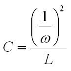 Eq. 16: Relationship Between Inductance, Capacitance, and Self-Resonant Frequency Using Eq. 16 the capacitance of the transformer is calculated to be X nF. This otherwise parasitic circuit element will also be used to help achieve lossless switching. Combining these measurements with previous calculations, a fairly complete model of the transformer can be assembled, as shown below. Fig. 29: Transformer Model Using identical methods the inductance, capacitance and SRF of the inductors can also be measured. The model for the inductors is shown below. Fig. 30: Inductor Model Resonant Circuit Design An important aspect of this design is the ability to eliminate switching losses by using the energy stored in parasitic inductive and capacitive elements of the circuit to create a resonant circuit which will allow the main switches to be turned on and off with no voltage across them, allowing lossless switching. Synchronous Rectification Circuit Design So far the current doubler rectifier has been shown with diodes as the rectifying elements; however, diodes typically have fixed voltage drops during conduction. If the diodes are replaced with MOSFETs with suitably low RDS_ON, the conduction voltage will be lower than the diode's forward voltage drop and less power will be dissipated. A synchronous rectifier does just this, by replacing the diodes with MOSFETS and controlling them to operate identically to the diodes they replace.
Additional Info - Read more about
synchronous rectification in the full bridge phase shifted topology here. [4]Simulation Simulating the circuit designs using the models developed so far will verify that the design works as intended. Testing The simulations have increased confidence in the design, but there is always the possibility of an effect that was not taken into consideration or large parameter deviations, so testing is necessary to prove the design. Files Here are all of the files used to design, test, and construct this converter. Everything from the high level spreadsheet, simulations files, to the board schematic and layout files and a bill of materials.
References [1] Andreycak, Bill, Phase Shifted, Zero Voltage Transition Design Considerations and the UC3875 PWM Controller, October 2010, http://www.ti.com [2] Balogh, Laszlo, The Current-Doubler Rectifier: An Alternative Rectification Technique for Push-Pull and Bridge Converters, October 2010, http://www.ti.com [3] Mappus, Steve, Current Doubler Rectifier Offers Ripple Current Cancellation, October 2010, http://www.ti.com [4] Mappus, Steve, Control Driven Synchronous Rectifiers in Phase Shifted Full Bridge Converters, October 2010, http://www.ti.com [ Back to Arcjet ] [ Back to Main ] Questions?
Comments? Suggestions? E-Mail me at MyElectricEngine@gmail.com
Copyright 2007-2010 by Matthew Krolak - All Rights Reserved. Don't copy my stuff without asking first. |